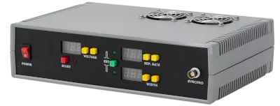
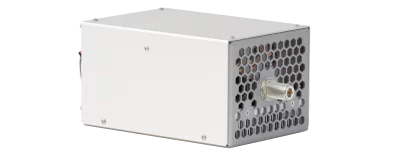
QBU-BT-series Pockels cell drivers


Applications
- Q-switching
- Pulse picking, pulse slicing
Features
- Highly tunable device
- Push-up, pull-down and mixed schemes in one module
- Up to 6 kV output voltage
- Up to 100 kHz and higher repetition rate
- Perfectly suits for the laboratory purposes
 Download manual (340 kB)
QBU-BT-series consists of several benchtop Pockels cell driver models that differ with output voltage range, max 6.0 kV bipolar (see also How to order? section). Please, note that bipolar device produces an output pulse voltage U by forming +U/2 at the positive output wire and –U/2 at the negative.
The main purpose of the QBU-BT driver is to control Pockels cells by applying a fast switching high voltage. The voltage level, operating frequency and pulse width can be selected in working range by user through RS-232 or through the front panel. Triggering is carried out automatically or via a signal from an external device.
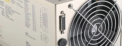
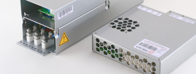
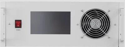
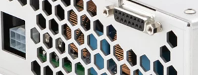
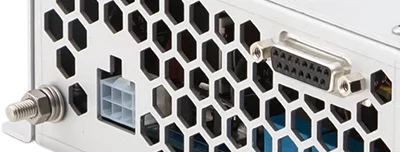
The devices have enclosures, so easy for the user to mount, they run on common 100-240 V AC 50/60 Hz, so, you don’t need extra power supply for the driver.
Three different operating modes are possible:
- push-up (= normally off scheme), when a base voltage level equals to zero, triggering is internal
- pull-down (= normally on scheme), when pulses from base bias voltage to ground are generated, triggering is internal
- triggering by an external low voltage arbitrary TTL signal, external synchronization mode.
The fact that the benchtop Pockels cell driver has a big number of settings, allowing an output signal customization in many ways to solve wide range of tasks, makes them very suitable to use in laboratory.

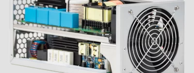
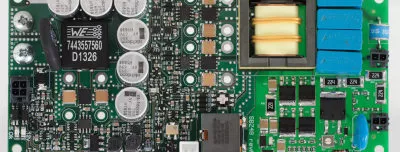
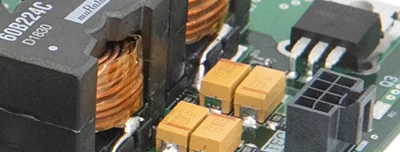
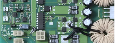
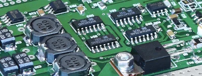
QBU-BT-series is based on MOSFET technology and offers high repetition rates and fast transition time (< 20 ns) for both pulse edges.
Performance
In internal synchronization mode the QBU-BT-series (from QBU-BT-1004 to QBU-BT-6024) performance is limited to values given in a table below. The total capacitive load of Pockels cell and connective cable is assumed to be 23 pF (this corresponds to 50 cm output cable bent in non-optimal way and higher than normal Pockels cell capacitance).
Even higher performance can be achieved in external synchronization mode and/or in a burst mode (i.e. for short term operations).
The performance deteriorates for higher load capacitance.
Please, also take a look at other our Pockels cell driver series, for example:
- up to 10 kV benchtop Pockels cell driver QBU-BT-10kV
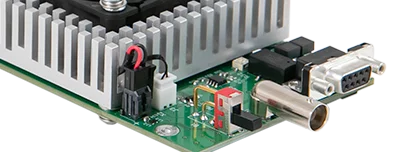
- up to 6 kV board QBU-series
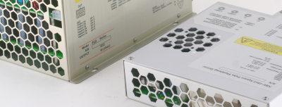
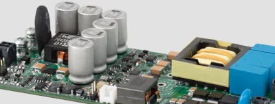
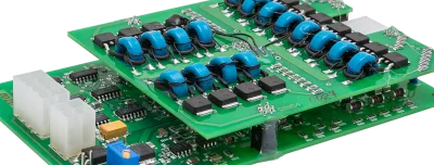
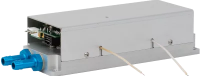
| QBU driver without case | Benchtop Q-switch driver | Compact driver, up to 4 kV |
 |
 |
 |
Input:
Output:
push-up scheme
triggering by an arbitrary external TTL signal
200 ns – ∞ (in external synchronization mode)
Environment:
Other:
2) 10-90% level, guaranteed at load capacitance 23 pF and below
Voltage modifications
Model *
Description
(*) Other output voltages are available on request
Other options
Example
Low jitter option
Download user manual (342kB)