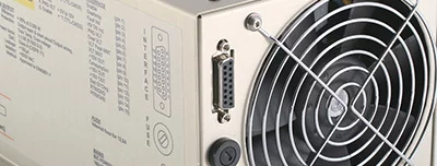
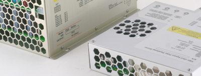
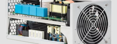
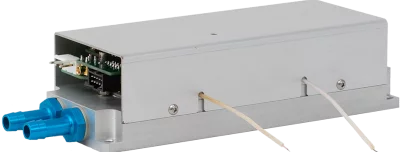
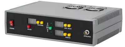
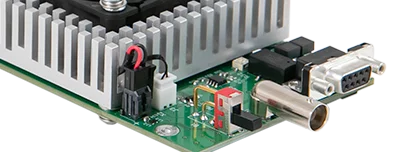
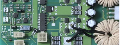
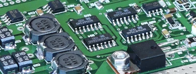
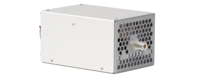
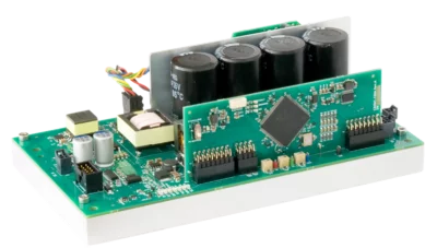
SDC-150A diode controller


Applications
- DPSS Nd:YAG pumping + q-switching
Features
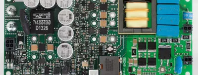
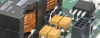
- The module consists of pulsed current source, TEC controller and Pockels cell driver (DKDP or LiNbO3)
- Input – 28±7 V DC
- Output diode current – up to 150 A, 25 V, 300 us, 30 Hz (but 20 W max)
- Pulse width – 50 – 300 us
- Repetition rate – up to 30 Hz
- Rise / fall time – < 50 us
- Modifications are possible
 Download manual (1 MB)
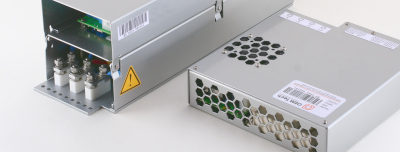
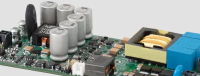
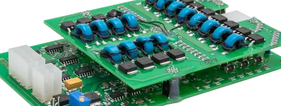
SDC-150A is a complete solution for powering and controlling a diode-pumped solid-state Nd:YAG laser. Our module includes a pulsed current source to drive pumping diodes, TEC controller for their thermal stabilization and embedded Pockels cell driver for generation of Q-switched pulses.
The module requires a 28 V DC (±7 V) power supply.
SDC-150A can be controlled either digitally via RS-232 interface or manually using jumpers and trimpots (stand-alone mode). Base interface is RS-232 (RS-485 is available as an option). Simple PC software is supplied together with the controller.
The module could be synchronized internally, when pulses are generated according to the internal clock, or externally, when pulses with user fixed width are triggered by external synchronization signal.
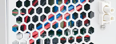
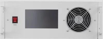
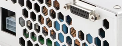
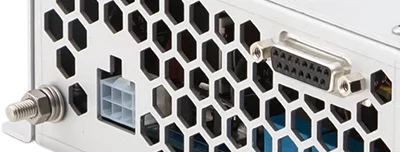
The cooling, when needed, is performed through the heatsink attached to the bottom surface.
Input:
Output 1 (diode driver, pulses to pumping diodes):
Load
Diode compliance voltage (Vmax)1
> 40 W on request (with derated operation temperature)
Output 2 (TEC):
Output 3 (Pockel cell driver, DKDP version):
Output 3 (Pockel cell driver, LiNbO3 version):
• From short-circuit at the outputs
• From overheating of internal components
• Interlock door connection
• Fault
• Synchro input
• Synchro output
Environment:
Other:
Many parameters of the SDC-150A can be taylored to your needs. Some of them are listed below:
- output voltage / current for diodes
- output voltage (Pockels cell driver)
- reduced or bursted output power
- interfaces
- type and location of connectors
Modifications
Model
Description
SDC-150A-25V
Base version:
- • 150 A maximum output current
- • 25 V maximum output voltage
- • Maximum output power > 20 W
(target regime 150 A, 25 V, 250 us, 20 Hz)
- • 110 A maximum output current
- • 85 V maximum output voltage
- • Maximum output power > 20 W
(target regime 110 A, 85 V, 220 us, 10 Hz)
- • 110 A maximum output current
- • 85 V maximum output voltage
- • Boosted output power; achieved by the cost of narrowed operating temperature range
- • Maximum output power > 40 W
(target regime 110 A, 85 V, 220 us, 20 Hz) - • Operating temperature 0 – 40 °C
Download user manual (1 MB)