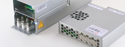
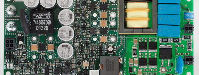
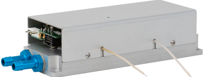
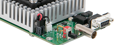

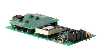
QBU-mini-SP Pockels cell drivers


Applications
- Q-switching
- Pulse picking, pulse slicing
Features
- Compact (as small as 102x50x20 mm)
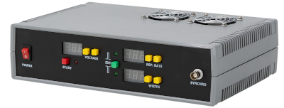
- Output is triggered by an arbitrary external TTL signal
- Up to 4.0 kV output voltage
- > 10 kHz repetition rate (4.0 kV, 7 pF)
- < 10 ns rise time and fall time
 Download manual (440 kB)
Pockels cell drivers QBU-mini-SP is a series of several Pockels cell driver circuit boards that differ with output voltage range (up to 4.0 kV bipolar), see also How to order? section. Modules produce bipolar high voltage pulses with high repetition rate, fast rise time and fall time (< 10 ns), adjustable voltage amplitude and pulse width (from 100 ns to 2000 ns).
The series is a modification of QBU-mini. The main differencies are:
| QBU-mini-SP | QBU-mini | |
| Pulse width, ns | 100 – 2000 | 200 -∞ |
| Rise / fall time, ns | < 10, typ. 7 | < 15, typ. 10 |
| Jitter, ns | ± 0.2 | ± 2 |
| Delay time, ns | < 40 | < 160 |
Please, note that by bipolar device an output pulse voltage U is formed by applying +U/2 to positive output wire and –U/2 to negative.
QBU-mini-SP series is specially designed to control Pockels cells by applying a fast switching high voltage. The modules require +24 V DC power supply and pulse generator to set an operating frequency and pulse width. An output voltage level can be programmed in working range by user either manually (through onboard configuration trimpot) or remotely (applying a DC voltage to the respective pin).
Triggering by an external low voltage arbitrary TTL signal allows modules to work in next scenarios:
- push-up (= normally off scheme), when a base voltage level equals to zero
- pull-down (= normally on scheme), when pulses from base bias voltage to ground are generated
- user-defined scheme, with arbitrary width and frequency of pulses.

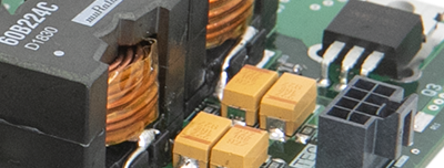
QBU-mini-SP series is based on MOSFET technology and offers high repetition rates and fast transition time (< 10 ns) for both pulse edges.
Kept cool enough with forced air cooling, at low load capacitance and low operating voltage modules may achieve tens of kHz performance (continuous mode) or nearly twice more (burst-mode). At the full load (4.0 kV, 7 pF) the repetition rate is higher than 10 kHz.
Input:
Output:
higher at lower load capacitances and voltages 1, 2
Environment:
Other:
2) forced air cooling is required for operating with high repetition rates
3) 10-90% level, guaranteed at load capacitance 7 pF and below
Modifications
Model *
Description
(*) Other output voltages are available on request
Example
Download user manual (440kB)