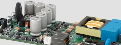
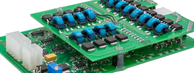
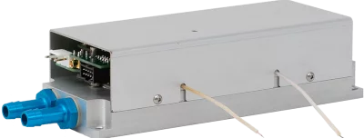
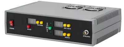
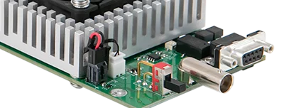
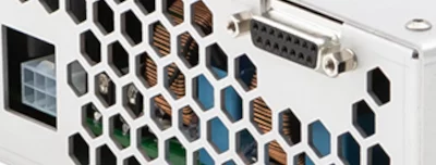
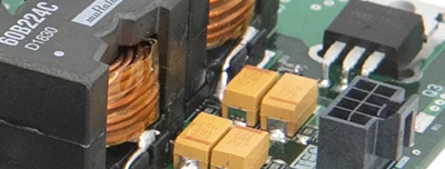
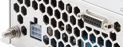
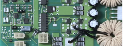
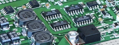
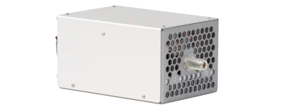
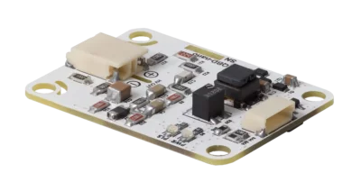
QBD-nano avalanche transistor Pockels cell driver
Applications
- Cavity dumping
- Q-switching
Features
- Compactness (40x30x10 mm)
- Bipolar output
- Up to 5 kV output voltage
- Up to 10 kHz repetition rate
- 1-3 ns rise time
QBD-nano is an extremely compact Pockels cell driver producing high voltage pulses with high repetition rates, fast rise time and adjustable pulse amplitude. Wide temperature range of operation is another important feature.
It produces an up to 5 kV bipolar output voltage. Please, note that by bipolar device an output pulse voltage U is formed by applying +U/2 to positive output wire and –U/2 to negative.
QBD-nano is specially designed to control Pockels cells by applying a fast switching high voltage. The module requires +5 …+12 V DC power supply and a pulse generator to set an operating frequency. An output voltage level can be programmed in 0.8-1 UMAX range by user either manually (through onboard configuration trimpot) or automatically (applying a DC voltage between respective pins).

Super-compact Pockels cell driver QBD-nano is based on avalanche transistors and offers fast transition time for a leading pulse edge. The recovery time by QBD-nano is relatively long (5-10 μs for the trailing pulse edge vs 1-3 ns by QBU-nano).
QBD-nano has some duration (on-time, “shelf”). It could be choosen at the time of order in 0.5-1 μs range. By default, it is 0.8-0.9 μs.
As alternative Q-switch driver, please kindly find:
QBD-series, up to 6 kV.
QBD-mini, compact version of QBD, up to 4 kV
Advanced Q-switch drivers are more improved, allow to change an output voltage level and advanced switching control to vary pulse repetition rate and width (long pulses, from 200 ns to CW). They provide pulses with both fast edges (< 15-20 ns) and allow to switch high voltage on the cryslal shortly before pull-down pulse to prolongate the crystal life-time.
QBU-series, up to 6 kV.
QBU-mini, compact version of QBU, up to 4 kV
QBU-mini-SP, compact version of QBU with short pulses, up to 4 kV QBU-10kV-series, up to 10 kV.
Input:
max 200 mA @ 12V
160-180 mA @ 12 V in target regimes:
5 pF, 5.0 kV, 2 kHz
5 pF, 3.8 kV, 4 kHz
5 pF, 2.5 kV, 8 kHz
Output:
2500 V, 3800 V, 5000 V, other on request, see also How to order? section
Environment:
Other:
2) depends on triggering signal parameters
3) depends on ambient temperature (maximal repetition rate is derated approximately twice at 65 °C ambient temperature and rises in cooler conditions)
QBD-nano-XXYY, where:
– XX codes the maximum output voltage (UMAX)
– YY codes the maximum repetition rate (FMAX)
Voltage modifications
Model
Description
FMAX= 2 kHz
High voltage version, 2kHz for 5pF at 5.0kV, 25 ̊C
UOUT= 2.8 – 3.8 kV
FMAX= 4 kHz
Base version, 4kHz for 5pF at 3.8kV, 25 ̊C
UOUT= 1.9 – 2.5 kV
FMAX= 8 kHz
Low voltage version, 8kHz for 5pF at 2.5kV, 25 °C
Other modifications are available on request.
Download user manual (0.6MB)
